Universal purpose optoelectronic logic element with input optical switching of AND/NAND, OR/NOR and XOR/XNOR functions
- PCB
- 2023-09-23 23:21:34
The optoelectronic logic element AND, OR and XOR is considered, the output signal of which can be inverted when the input control signal is applied, thereby converting the logic element into NAND, NOR and XNOR.
Among the assortment of logic chips, there are known chips whose power can be turned on or off by feeding a control signal to one of the inputs of the chip.
The principle of creating a universal optoelectronic logic element with input optical switching of AND/NAND, OR/NOR and XOR/XNOR functions will be discussed below.
Wow the engineering world with your unique design: Design Ideas Submission Guide


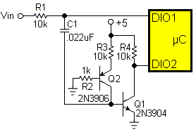
The optoelectronic logic element, Figure 1, contains three input control switches of optoelectronic pairs U1.1, U2.1 … U6.1 (optronic pairs are highlighted in color for clarity), made on transistors Q1, Q3 and Q5.
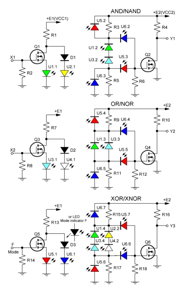
Figure 1 Optoelectronic logic element of universal purpose with optical switching of output functions.
In the absence of input signals, current flows through the LEDs of the optocoupler pairs U2.1, U4.1 and U6.1. When high-level signals are applied to the inputs X1, X2 and F (Mode), the optocouplers switch: current flows through the LEDs of the optocouplers U1.1, U3.1 and U5.1.
When high-level signals are applied to the inputs X1, X2 or F (Mode), the optocoupler pairs switch: current flows through the LEDs of the optocoupler pairs U1.1, U3.1 or U5, respectively, to the input signal.
The receiving part of the logic element contains photodiodes of optocouplers, resistors, as well as output stages on transistors Q2, Q4 and Q6.
When the “Log. 1” and/or “Log. 0” level signals are applied to the control inputs X1, X2 or F (Mode), the signals at the outputs Y1 AND, Y2 OR and Y3 XOR change in accordance with Table 1.

Table 1Truth table of a universal purpose optoelectronic logic element with optical switching of output functions.
Another simpler version of the implementation of a universal purpose optoelectronic logic element with an input optical switching of functions is shown in Figure 2.

Figure 2 A simpler implementation of a universal purpose optoelectronic logic element with an input optical switching of functions.
The input and receiving parts of the device can be powered from separate power sources (to provide galvanic isolation of input and output) or a single power source.
Such an optoelectronic logic element can be placed in a conventional case DIP10, Figure 3.

Figure 3 Possible type of the housing of a universal optoelectronic logic element chip.
For a visual indication of the involved input F, instead of the diode D3, an LED (Mode indicator) shown in Figures 1 and 2 can be used.
Michael A. Shustov is a doctor of technical sciences, candidate of chemical sciences and the author of over 750 printed works in the field of electronics, chemistry, physics, geology, medicine, and history.
Related Content
Universal purpose optoelectronic logic elementsUniversal logic element on one transistor and its applicationsImproved comparators distinguish between A = B = 0 and A = B = 1 states to enable better designsRFL-class logic gatesUniversal purpose optoelectronic logic element with input optical switching of AND/NAND, OR/NOR and XOR/XNOR functions由Voice of the EngineerPCBColumn releasethank you for your recognition of Voice of the Engineer and for our original works As well as the favor of the article, you are very welcome to share it on your personal website or circle of friends, but please indicate the source of the article when reprinting it.“Universal purpose optoelectronic logic element with input optical switching of AND/NAND, OR/NOR and XOR/XNOR functions”