How different isolated bias supply topologies impact EMI
- Analog
- 2023-09-23 21:19:17
Small, isolated power supplies provide power across isolation barriers in applications from electric vehicle traction inverters to factory control modules. In this Power Tip, I’ll examine different isolated bias-supply topologies and their electromagnetic interference (EMI) performance. As you’ll see, parasitic capacitance across the isolation transformer is a major contributor to common-mode noise propagation.
In traction inverters, gate drivers actuate the high-power switches—usually insulated-gate bipolar transistors (IGBTs) or silicon carbide (SiC) MOSFETs—which convert energy between the high-voltage battery and the electric machine (see Figure 1). The gate drivers are typically isolated, with one part of the gate driver IC connected to the low-voltage domain (the primary side) and another part connected to the high-voltage domain (the secondary side). The gate-drive control signals come from a microcontroller on the primary side and are passed through to the secondary side to turn the power switch on and off.
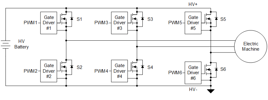
Figure 1 A traction inverter with isolated gate drivers. Source: Texas Instruments


The secondary side of the isolated gate driver needs an isolated power supply in order to actuate power switch turn-on and turn-off (see Figure 2).

Figure 2 An isolated bias supply provides power across the isolation barrier for the isolated gate driver. Source: Texas Instruments
The power ratings for isolated bias supplies are usually fairly low—less than 10 W. The equation below estimates their power requirements as:
PDRV = VDRV x Qg x FSW (1)
where VDRV is the gate-drive voltage, Qg is the switch gate charge, and FSW is the switching frequency of the switch (not the isolated bias-supply switching frequency). The gate-drive voltage depends on which switch you select, but typically ranges from +15 V to +25 V on the positive rail and –8 V to 0 V on the negative rail.
Common topologies for isolated bias supplies include flyback, push-pull and inductor-inductor-capacitor (LLC). Some fully integrated power modules (that include the transformer in the package) use a full-bridge configuration on the primary side. Flyback converters, such as the LM5180-Q1 from Texas Instruments (TI), are well known, provide good output voltage regulation, are fairly efficient, can be designed without an optocoupler (using primary-side regulation), and can have multiple isolated outputs. Their drawbacks are that they tend to be limited in frequency range (<350 kHz) and have a large transformer size. Push-pull converters, such as TI’s SN6507-Q1 and LLC converters, such as TI’s UCC25800-Q1, are simple but do not have closed-loop feedback. As a result, the output voltage regulation suffers, potentially requiring a pre-regulator, a post-regulator, or both. Integrated power modules (such as TI’s UCC14341-Q1) can regulate the output voltage and are simple and small, but their drawbacks are limited power output (typically <1.5 W) and lower efficiency than alternative options.
One question you may have is about the EMI performance of different topologies: Do certain topologies have more or less impact on electromagnetic compatibility results? To address these questions, let’s first examine the isolation transformer. Some parasitic capacitance does exist between the windings of the transformer, which charges or discharges when the traction inverter switch node (VSW) switches between HV+ and HV– nodes. A short pulse of common-mode current charges or discharges the parasitic capacitance during the switching transition. The common-mode current is directly proportional to the parasitic capacitance and the switch-node slew rate (dv/dt). Large capacitance or faster switch-node slew rates—as you might see with wide band-gap semiconductors such as gallium nitride (GaN) and SiC—will result in more common-mode current. Figure 3 highlights this parasitic capacitance and the common-mode current used to charge and discharge it.

Figure 3 Common-mode current charges the transformer parasitic capacitance when the switch node (VSW) transitions. Source: Texas Instruments
Converter topology does influence transformer design and the resulting parasitic capacitance. Flyback converter transformers (or coupled inductors if you prefer that nomenclature) are designed to have strong coupling between the primary and secondary sides in an effort to reduce leakage inductance. Leakage inductance causes unwanted voltage spikes and power loss in snubber circuits. The unfortunate impact of designing for low leakage inductance is that the interwinding capacitance typically increases, and can be 20 pF or more. On the other hand, it is possible to design LLC converters to use a transformer’s leakage inductance in its resonant tank. As a result, you would not need to design the transformers to minimize leakage inductance; they can have a parasitic capacitance around 2 pF. As you’ll see, this helps reduce common-mode currents.
Table 1 shows some parameters from a study of four isolated bias topologies to experimentally validate the impact of transformer parasitic capacitance on common-mode current. All of the converters were designed for a 15-VIN, 15-VOUT, 1.5-W application. The switching frequency of each topology is based on typical values, with the transformers designed accordingly. As you can see, the flyback converter transformer has the lowest leakage inductance and the highest parasitic capacitance. The LLC converter transformer has the highest leakage inductance and the lowest parasitic capacitance.

Table 1 Transformer parameters for four example isolated bias-supply converters. Source: Texas Instruments
Comparing these isolated bias-supply topologies involved performing an extensive set of tests: efficiency, load regulation, input and output ripple, thermals, and conducted and radiated EMI. To focus on the common-mode current measured between the isolated grounds in the system, my colleagues connected a wire between the two grounds and measured the common-mode current when the high-power switches (in this example, a GaN half bridge using the LMG3522R030-Q1) turned on and off at 400 V. Figure 4 and Figure 5 show the results for a high-voltage switch-node slew rate of 40 V/ns and 100 V/ns, respectively.

Figure 4 Common-mode current comparison at a 40-V/ns slew rate on the switch node. Channel 1 is the high-voltage switch node (200 V/div) and Channel 2 is the common-mode current (500 mA/div). Source: Texas Instruments

Figure 5 Common-mode current comparison at a 100-V/ns slew rate on the switch node. Channel 1 is the high-voltage switch node (200 V/div) and Channel 2 is the common-mode current (500 mA/div). Source: Texas Instruments
The measured results demonstrate that the common-mode current for the flyback transformer was the largest (935 mA and 1,420 mA for 40-V/ns and 100-V/ns slew rates). This is to be expected, since the transformer had the largest parasitic capacitance. And because the LLC converter had the lowest parasitic capacitance, the common-mode current measured was the smallest (197 mA and 570 mA for 40-V/ns and 100-V/ns slew rates). Large common-mode current spikes are detrimental, since they can conduct noise from the high-voltage domain to the low-voltage domain, cause ground bounce; and potentially lead to poor converter operation including skipped pulses, lost regulation, or unexpected shutdowns.
Common-mode currents can be especially difficult to mitigate. One of the best ways to address common-mode current issues is to avoid generating common-mode current in the first place. While the application discussed here was a traction inverter in an electric vehicle, the principles apply to applications such as grid-connected converters and server power supplies.
Pradeep Shenoy leads the Power Design Services team at TI, focused on automotive systems. He previously worked in TI’s Kilby R&D Lab and in the Switching Regulators business unit. He has presented technical and industry presentations at the Applied Power Electronics Conference nearly every year since 2011, and serves as general chair in 2023. He received the Illinois International Graduate Achievement Award in 2010, the Jack Kilby Award for innovation in 2015, and the Institute for Electrical and Electronics Engineers (IEEE) Richard Bass Award in 2020. He serves actively in the IEEE Power Electronics Society as treasurer. Shenoy has a Ph.D. from the University of Illinois Urbana-Champaign.
Acknowledgments
Prashant Kumar and Markus Zehendner completed the hardware design and testing.
Related Content
Power Tips #119: How to characterize a power transformer for EMI performancePower Tips #118: Using interleaved ground planes to improve noise filtering from isolated power suppliesPower Tips #117: Measure your LLC resonant tank before testing at full operating conditionsPower tips #116: How to reduce THD of a PFCPower Tips #115: How GaN switch integration enables low THD and high efficiency in PFCAdditional resources
Flyback Transformer Design Considerations for Efficiency and EMIIsolated Gate-Driver Bias-Supply Design ConsiderationsHow different isolated bias supply topologies impact EMI由Voice of the EngineerAnalogColumn releasethank you for your recognition of Voice of the Engineer and for our original works As well as the favor of the article, you are very welcome to share it on your personal website or circle of friends, but please indicate the source of the article when reprinting it.“How different isolated bias supply topologies impact EMI”